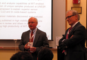


Scientists at Unesp and MIT synthesize and test nanostructured oxide semiconductors for use in gas sensors for environmental control and monitoring (Harry Tuller, left, and José Varela)
Scientists at Unesp and MIT synthesize and test nanostructured oxide semiconductors for use in gas sensors for environmental control and monitoring.
Scientists at Unesp and MIT synthesize and test nanostructured oxide semiconductors for use in gas sensors for environmental control and monitoring.

Scientists at Unesp and MIT synthesize and test nanostructured oxide semiconductors for use in gas sensors for environmental control and monitoring (Harry Tuller, left, and José Varela)
The discovery of two semiconductor materials structured on a nanometric scale (one billionth of a meter) – copper oxide and tin oxide – with high sensitivity and selectivity in detecting polluting gases in the atmosphere, may be used to develop sensors for environmental control and monitoring. The announcement was made today, October 22, during the second symposium of FAPESP Week 2012, held at the Massachusetts Institute of Technology (MIT) in Boston.
The outcome is fruit of the project “Advances in nanostructured semiconducting oxides for gas sensors,” conducted by research teams led by Professors José Arana Varela of the Chemistry Institute at the São Paulo State University (Unesp) in Araraquara, and Chief Executive Officer of the FAPESP Executive Board, and Harry Tuller of the Department of Materials Science and Engineering of MIT.
“In addition to the nanometric scale, which offers semiconductors greater sensitivity, other factors are also important in defining these materials,” says Professor Varela. “Some of the tests performed at MIT show that different ways of structuring semiconductor particles can lead to significant changes in electrical conductivity and thus modify the response of the materials when they come into contact with gases. That’s why our next step will be to explain why the morphology is so relevant to this process.”
Cooperation between the two research groups has been complemented by the expertise and laboratory infrastructure each team provides. According to Varela, the team established at Unesp upon creation of the Multidisciplinary Center for Development of Ceramic Materials (CMDMC) – one of FAPESP’s Research, Innovation and Dissemination Centers (RIDC) – in Araraquara in 2001, has a large capacity for synthesizing materials and preparing samples. At MIT, Harry Tuller’s team has extensive experience with nanosensors, the ability to characterize the materials, and a very well-controlled system for analyzing eight samples at a time.
“Synergy is the key word that describes our collaboration,” says Professor Tuller. “Personal interactions and the capacity for mutual transfer of specific expertise between the two groups, allowing, in just a short period of time, real advances to be made with regard to the type of materials developed and interpretation of the phenomena, has opened up new avenues of research.”
Since early 2011, this integration between teams from the two countries has been productive. One article has already been published in the high impact journal Advanced Functional Materials and others are in the final stages of preparation and editing.
Republish
The Agency FAPESP licenses news via Creative Commons (CC-BY-NC-ND) so that they can be republished free of charge and in a simple way by other digital or printed vehicles. Agência FAPESP must be credited as the source of the content being republished and the name of the reporter (if any) must be attributed. Using the HMTL button below allows compliance with these rules, detailed in Digital Republishing Policy FAPESP.


