


One of the possible applications of this material is the production of TV screens capable of emitting more light and consuming less energy. A Brazilian researcher participated in the research project conducted at Los Alamos National Laboratory (Nature Communications)
One of the possible applications of this material is the production of TV screens capable of emitting more light and consuming less energy. A Brazilian researcher participated in the research project conducted at Los Alamos National Laboratory.
One of the possible applications of this material is the production of TV screens capable of emitting more light and consuming less energy. A Brazilian researcher participated in the research project conducted at Los Alamos National Laboratory.
One of the possible applications of this material is the production of TV screens capable of emitting more light and consuming less energy. A Brazilian researcher participated in the research project conducted at Los Alamos National Laboratory (Nature Communications)
By José Tadeu Arantes
Agência FAPESP – LEDs (light-emitting diodes) have become omnipresent in the contemporary life. They are used in TV screens, computer monitors, signage, traffic lights, cars and remote controlled devices, to mention a few of their many applications. They consist basically of semiconductors that are connected to an energy source and emit light when the electrons in the current recombine with the existing gaps in the atomic network of the material, releasing energy in the form of photons.
So-called quantum dots, consisting of nanometer-size particle semiconductors, are excellent materials for manufacturing LEDs because they produce intense light; emit light at a very narrow wavelength, which makes high color resolution possible; and are relatively cheap for large-scale production. Still, there is one powerful factor limiting their use: their low electrical efficiency, as little as 0.1% or 0.2%.
This low efficiency results from a quantum phenomenon known as the Auger effect, named for one of the people who discovered it, French physicist Pierre Victor Auger (1899-1993).
When an electron near the atomic nucleus is removed, it leaves an inner-shell vacancy in the electron cloud around the nucleus. Another, more distant electron (endowed with a higher level of kinetic energy) then fills the vacancy created by the removal of the first electron.
The expected effect is that the electron’s excess energy is released by the emission of a photon (a particle associated with electromagnetic interaction). However, the energy could instead be transmitted to a third electron, placing it in a state of excitation. The third electron then overcomes the nucleus’ electromagnetic attraction and is ejected by the atom. This latter scenario is what is known as the Auger effect.
An analogous phenomenon (in this case Auger recombination) can occur in a semiconductor when an electron occupies a gap in the atomic network instead of releasing a photon. The electron transmits its energy to another electron, which is ejected from the network. Transforming electrical energy into kinetic energy, instead of luminous energy, the Auger recombination makes the efficiency of LEDs extremely low.
But a recent experiment, conducted in the Chemistry Division of Los Alamos National Laboratory, in the United States, managed to control the influence of Auger recombination. The team of researchers, including Brazilian Lázaro Padilha, a faculty member at the Universidade Estadual de Campinas’ Gleb Wataghin Physics Institute (Unicamp), published their research in Nature Communications - the article can be accessed at: www.nature.com/ncomms/2013/131025/ncomms3661/full/ncomms3661.html.
“We produced new materials that can minimize the Auger effect. With them, it is possible to obtain LEDs that are 10 times more efficient, with an electrical energy conversion rate around 2%,” said Padilha.
“More than this, we managed to limit the process of ionization of the material. This ionization, which occurs as a result of the injection of electrons, accentuates the Auger effect. The greater the injected charge, the greater the Auger effect. By creating a barrier to control the injection, we reached 8% efficiency. Effectively, we increased the efficiency 40-fold, from 0.1% or 0.2% to 8%,” added the researcher.
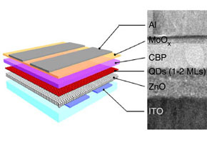
For this purpose, the researchers utilized cadmium selenide dots (CdSe) as the starting point. This semiconductor material gives the LED its 0.1% to 0.2% efficiency. By coating the cadmium selenide nucleus of each particle with a layer of cadmium sulfate (CdS) and introducing a very fine alloy of the two materials (CdSeS) between the CdSe nucleus and the external layer of CdS, it was possible to increase the efficiency to approximately 2%.
Another layer composed of a zinc, cadmium and sulfur alloy (ZnCdS) was then added to the CdS layer. This alloy works as a barrier, limiting and controlling the entry of electrons to the nanoparticles and, in this manner, reducing the Auger effect. With this approach, it was possible to increase the efficiency to 8%.
“The distinguishing merit of this work was the materials engineering, which made it possible to control the interaction of the electrons in the current with the gaps (i.e., lack of electrons) in the atomic network of the semiconductor,” commented Padilha.
“The nanoparticles, with a total diameter of 7 nanometers each, were obtained through chemical synthesis, with rigorous control at each stage of the reactions,” he explained.
“With the utilization of modified nanoparticles, it will be possible, for example, to produce TV sets that can generate more light with lower electricity consumption. Another advantage – related to the use of quantum dots in general – is that the narrow band of luminous emission of each nanoparticle will greatly improve the color resolution”.
The Agency FAPESP licenses news via Creative Commons (CC-BY-NC-ND) so that they can be republished free of charge and in a simple way by other digital or printed vehicles. Agência FAPESP must be credited as the source of the content being republished and the name of the reporter (if any) must be attributed. Using the HMTL button below allows compliance with these rules, detailed in Digital Republishing Policy FAPESP.
