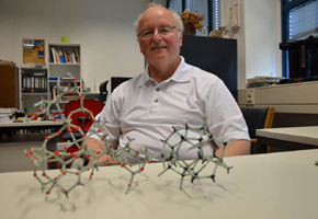


Harry Tuller, of MIT, was one of the keynote speakers in João Pessoa, Brazil (Helmholtz Zentrum Berlin)
Harry Tuller, of MIT, was one of the keynote speakers in João Pessoa, Brazil.
Harry Tuller, of MIT, was one of the keynote speakers in João Pessoa, Brazil.

Harry Tuller, of MIT, was one of the keynote speakers in João Pessoa, Brazil (Helmholtz Zentrum Berlin)
By José Tadeu Arantes, João Pessoa
Agência FAPESP – One prospect for the relatively near future is that a single device, such as a cellphone, will be used to control multiple day-to-day functions: to turn on and off lights or the television, to pay for supermarket purchases or to go through a subway turnstile.
This scenario, which is one part fiction and many more of science, was informally described by physicist José Arana Varela, full professor at Universidade Estadual Paulista at the Araraquara Campus (Unesp -Araraquara) and FAPESP CEO, during one of the breaks in the 6th International Conference on Electroceramics, held from November 9 to 13 in João Pessoa, Paraíba. “Memory will be a central factor. Connected to different circuits, a single device could conduct multiple functions. And this memory will be composed of electroceramic material,” said Varela.
The presentation conducted during the event validates Varela’s prediction because research is highly advanced in this area. Professor Harry Tuller of Massachusetts Institute of Technology (MIT) created the International Conference on Electroceramics in 2003. MIT hosted the first conference, which has been held in odd-numbered years ever since. In addition to the United States, the conference has been held in South Korea, Tanzania, India, Australia and, now, Brazil.
The Brazilian Materials Research Society sponsored the event along with FAPESP, the National Council of Scientific and Technological Development (CNPq) and the Brazilian Federal Agency for the Support and Evaluation of Graduate Education (Capes). Reginaldo Muccillo, researcher at the Institute of Energy and Nuclear Research (IPEN), and Jose Antonio Eiras, associate professor at Universidade Federal de São Carlos (UFSCar), coordinated the event.
“We brought approximately 60 high-level researchers from the United States, Europe, China, Canada, Australia, India and other areas to João Pessoa, creating an excellent opportunity for interaction among researchers and Brazilian students,” affirmed Muccillo.
In addition to Harry Tuller, other noted speakers were Sossina Haile, of the California Institute of Technology (Caltech); Ramamoorthy Ramesh, of the University of California-Berkeley; Augusti Sin Xicola, of Pirelli&C Eco Technology in Italy; and Enrico Traversa, of King Abdullah University of Science and Technology in Saudi Arabia.
The topics covered are new, and the concept of electroceramics is something very recent. “Ceramics have been utilized by humanity for thousands of years. They are extremely stable and heat-resistant materials. There are many roles that they are capable of playing because of their chemical, mechanical and thermal characteristics,” affirmed Tuller. “However, until the past 50 years, no one cared about their electrical characteristics. This interest was sparked by the development of the electronics and microelectronics industry.”
“The people involved in these industries realized that they needed certain characteristics that cannot be met with conventional ceramics. It was based on this that the development of electroceramics emerged – not only the manufacture of standard electronic equipment but also, and increasingly, to fulfill many other functions,” added the MIT researcher.
“The peculiarity of electroceramics is that they respond in some manner or another to the presence of an electromagnetic field, presenting variations in electrical resistance, in magnetic permeability or in other electric or magnetic parameters,” explained Muccillo.
This classification primarily encompasses the semiconductor oxides of metallic elements, such as zirconium, tin or cerium, among others. “Because of their characteristics, they can be utilized as sensors (depending on the variations in the concentration of a given gas on the oxide surface, they have their electrical resistance proportionally modified so that the value of the resistance makes it possible to determine the concentration of gas even if it is extremely small), in the alternative production of energy (in photovoltaic cells that change light into electricity or drive fuel cells) or in the manufacture of ferroelectric memory (currently used in smartcards),” explained the IPEN researcher.
“Evolution in the sector has been super-accelerated. The electroceramics sector that we know today is very different from that of 10 years ago, when the first International Conference on Electroceramics was held. Today, we are talking about embedded technologies – embedded in a silicon chip, adding new functionalities,” commented Varela.
Miniaturization
In the presentation at the beginning of the Conference, Tuller highlighted two apparently opposite but complementary trends: what he called the “race to the bottom,” with manufacture of increasingly smaller devices, currently a few nanometers in size, and what he called the “race to the top,” with the production of increasingly larger liquid crystal displays on computers, TVs and illuminated signage.
“The big revolution in recent years, which should intensify over the next few years, is that sensors, which were previously large and heavy, were and continue being miniaturized and integrated into a single chip with multiple functions. The demand is for smaller devices, capable of integrating more and more functions that are accessible and cheap. Simultaneously, we are seeking displays and panels for capturing increasingly higher volumes of solar energy,” said Tuller.
According to the researcher, the process of miniaturization is so intense that the density (quantity of mass per unit volume) of the equipment doubles every 18 months. Meanwhile, this LCD technology turned over US$110 billion in 2012.
We are, therefore, close to the limit in both one sense and the other. “The process of miniaturization cannot be extrapolated indefinitely. We need to evolve to new concepts. And today, there are several studies in this regard. At the same time, because of the incredible success of the LCD technology, there is a need and the possibility of even greater development, perhaps of another magnitude employing electroceramics instead of liquid crystals,” affirmed Tuller.
One property of electroceramics that receives significant attention, according to Varela, is called “restrictive memory” – the property that the electrical resistance of the material, which varies according to the applied voltage, does not return to the same value when the voltage is withdrawn. This double resistance value – before and after voltage is applied – creates a binary capability. And binary devices can support data storage.
“Restrictive memory makes semiconductor oxides strong candidates for manufacturing nanostructured devices with high-density data storage, capable of integrating all microelectronics. This is the memory that is being studied at the moment and could cause a new revolution in microelectronics. This memory, which is sufficiently large and stable, can alone integrate the functions of an enormous number of circuits,” said Varela.
“Understanding this restrictive memory offers a large challenge to physicists. We need to understand the quantum physics of these systems whose dimensions are still close to an atomic scale. We know that the phenomenon exists, but without an in-depth understanding it will be impossible to reach reproducibility. We need to be capable of producing millions of parts, all with very small variations in the properties,” he affirmed.
More information about the conference is available at: www.ice2013.net.
Republish
The Agency FAPESP licenses news via Creative Commons (CC-BY-NC-ND) so that they can be republished free of charge and in a simple way by other digital or printed vehicles. Agência FAPESP must be credited as the source of the content being republished and the name of the reporter (if any) must be attributed. Using the HMTL button below allows compliance with these rules, detailed in Digital Republishing Policy FAPESP.


