


Figure (a): schematics of grating nanostructures in gold thin film on tellurite glass as substrate. Figure (b): experimental setup where polarized white light source illuminated samples from above and transmission spectra were recorded in detector (image: Scientific Reports)
A study conducted at a FAPESP-supported research center shows that light interacting with free electrons in a metal can traverse nanometric structures far smaller than its wavelength.
A study conducted at a FAPESP-supported research center shows that light interacting with free electrons in a metal can traverse nanometric structures far smaller than its wavelength.
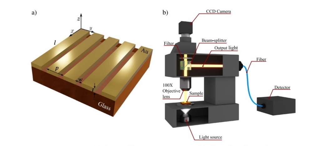
Figure (a): schematics of grating nanostructures in gold thin film on tellurite glass as substrate. Figure (b): experimental setup where polarized white light source illuminated samples from above and transmission spectra were recorded in detector (image: Scientific Reports)
By José Tadeu Arantes | Agência FAPESP – Moving electrons can be used to transport information down metal wires, but the transmission rate is limited owing to losses that occur on the way. The introduction of optical fibers reduced these losses while permitting much faster transmission rates. Broadband, which revolutionized the internet by bundling together telecommunications, radio and television, was made feasible by fiber optics. Now electronic circuits are being replaced by optical circuits to achieve faster data processing speeds.
The challenge is that electromagnetic radiation cannot cross or be guided by structures smaller than its wavelength, which is only a few micrometers (1 millimeter = 1,000 micrometers).
“A highly promising alternative is to create hybrid systems based on the interaction between light and ions. Our study showed that ions, quantum emitters, can interact with light via a metallic structure at the nanometric scale,” said physicist Euclydes Marega Júnior, a professor at the University of São Paulo’s São Carlos Institute of Physics (IFSC-USP) in Brazil.
The study was conducted at the Optics and Photonics Research Center (CEPOF), one of the Research, Innovation and Dissemination Centers (RIDCs) funded by FAPESP. It was also supported by a doctoral scholarship awarded to Gaston Lozano Calderón, whose research Marega supervised. The results are described in an article published in Scientific Reports.
“The phenomenon we observed and report in the article shows that nanometric photonic circuits can become a reality in the relatively near future, impacting current technologies and making nanometric transmission and processing of information possible at frequencies on the order of terahertz [1012 Hz]. This could produce a processing revolution equivalent to the photonics revolution in the field of information transmission,” Marega said.
Surface wave
The study permitted observation of the interaction between electromagnetic radiation and erbium ions near a very small metallic apparatus with a grating of slits. The structure’s order of magnitude was far smaller than the light wavelength, so that it could not be traversed by electromagnetic radiation without the aid of the light’s interaction with free electrons in the metal, creating surface plasmon polaritons, a type of surface wave with a shorter wavelength than light at the same frequency.
A plasmon is a quantum of plasma oscillation. Just as light consists of photons, the oscillation consists of plasmons. Polaritons are quasi-particles formed when photons couple strongly with excitons. They are half-light (photon) and half-matter (excitons).
In surface plasmon polaritons, surface waves are formed by the motion of charges in the metal (plasmons) and electromagnetic radiation in the air or dielectric (polaritons). “Confinement enables the electromagnetic radiation to interact with objects at this tiny scale,” Marega said.
Far away from the structure, radiation-ion coupling is weak, but very intense coupling is observed near it, along with additional phenomena such as Fano resonance, which occurs when two quantum systems, ions and radiation fields, interact.
The Fano effect is named after Italian-American physicist Ugo Fano (1912-2001), who in 1961 offered a theoretical explanation for electron scattering by helium. The phenomenon had previously been described by Ettore Majorana (1906-?), considered one of the greatest scientific minds in history. He disappeared aged 32 under mysterious circumstances and was never seen again.
According to Marega, the results of the study pertain to nanophotonics, an increasingly important research field with technological applications that are considered highly promising. The phenomena involved occur at a scale halfway between the atomic and photonic. A nanometer (nm) is equal to one-thousandth of a micrometer. Ten hydrogen atoms laid side by side would be 1 nm in width, for example.
Besides the IFSC-USP group, the investigation also involved researchers at two other Brazilian institutions – the Federal University of Piauí (UFPI) and the Federal University of São Carlos (UFSCar) – as well as Laval University in Canada and the National University of San Marcos in Peru.
The article “Demonstration of multiple quantum interference and Fano resonance realization in far-field from plasmonic nanostructure in ER3+ doped tellurite glass” is at: www.nature.com/articles/s41598-022-08858-x.pdf.
The Agency FAPESP licenses news via Creative Commons (CC-BY-NC-ND) so that they can be republished free of charge and in a simple way by other digital or printed vehicles. Agência FAPESP must be credited as the source of the content being republished and the name of the reporter (if any) must be attributed. Using the HMTL button below allows compliance with these rules, detailed in Digital Republishing Policy FAPESP.
