


Group led by João Antonio Martino of USP is developing transistor prototype that paves the way for the manufacture of electronic devices that are smaller and have more processing capacity
Group led by João Antonio Martino of USP is developing transistor prototype that paves the way for the manufacture of electronic devices that are smaller and have more processing capacity.
Group led by João Antonio Martino of USP is developing transistor prototype that paves the way for the manufacture of electronic devices that are smaller and have more processing capacity.
Group led by João Antonio Martino of USP is developing transistor prototype that paves the way for the manufacture of electronic devices that are smaller and have more processing capacity
By Karina Toledo, from Salamanca
Agência FAPESP – The emergence of a new type of transistor, known as FinFET or 3D transistor, could revolutionize electronics and pave the way for a new generation of computers, smartphones, tablets, televisions and other devices that are smaller and lighter, but have more processing capacity.
A group of researchers led by João Antonio Martino of the Polytechnical School of the University of São Paulo (USP) was able to design and fabricate a prototype of the device for the first time in Brazil.
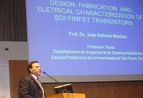
The announcement was made this Wednesday (12/12) during the “Frontiers of Science – Brazil and Spain in the 50 years of FAPESP” event.
The “Frontiers of Science” event includes the celebration of 50 years of FAPESP in the cities of Salamanca (12/10-12/12) and Madrid, 12/13-12/14), and brings together researchers from the state of São Paulo and from several academic and research institutions of Spain in a lively and varied program that is open to the public.
“All electronic devices have circuits formed by transistors connected for a specific purpose. The better the transistor, the better the circuit, in other words, the greater processing capacity and memory,” Martino told Agência FAPESP.
Made basically of silicon – which acts as a semiconductor base – metal and insulators, this electronic component serves to amplify or switch electrical signals.
Traditional models are assembled and interconnected horizontally, leaving gates for the passage of electric current only on top. The FinFETS type of transistor, besides being considerably smaller in size, is arranged vertically.
“Besides allowing more transistors to be placed within the same area of silicon, the vertical arrangement enables placing gates for electric current to pass on the two sides and across the top. This more than doubles the processing capacity,” Martino said.
Research groups from several countries have spent the past decade developing the technology to fabricate these components. In 2012, Intel launched the line of Ivy Bridge line of processors, the first commercial product to use 3D transistor technology.
“Now Brazil also holds this technology. In November, we were able to fabricate the first FinFETS developed completely in Brazil,” Martino said.
The study has received funding from FAPESP and a partnership of scientists from the State University of Campinas (Unicamp) and the FEI University Center.
The Thematic Project began in 2009, but before that, the group had already begun to study the operation of 3D transistors fabricated abroad.
“First we had to understand their electrical behavior. Then we had to study how they reacted to special conditions like high temperatures, low temperatures or radiation. All of this was necessary to determine which applications were possible for this type of component. Only then did we begin to try to fabricate it,” Martino said.
Partnership with industry
The objective now is to begin a new project to try to produce a Brazilian prototype that measures 50 nanometers (nm) in width, 100 nm in height and 1,000 nm in length. For comparison purposes, the thickness of a single strand of hair is approximately 80,000 nm.
Martino goes on to say “It is still a simplified version with only three layers. The Intel circuits have 15 - 20 layers. But starting from this prototype, we can take it as far as we need to.”
The researcher explained that the layers determine the layout of the transistor’s material components. “A transistor is made from a combination of semiconductor, metal and insulator. The mask, a rather sophisticated and expensive photographic process, is used to give it the design and determine where each layer goes.”
Martino went on to explain that the process had to be simplified in order to obtain the first devices. “I don’t know of any other group that has made a transistor of such complexity using such a small number of masks. This is also difficult.”
The next step, according to the researcher, is to perfect the FinFET model. He pointed out that, “for the time being, it is still being developed at the university. We have gone as far as possible at the research level. Now we need an industry partnership to develop a model for commercial use.”
The Agency FAPESP licenses news via Creative Commons (CC-BY-NC-ND) so that they can be republished free of charge and in a simple way by other digital or printed vehicles. Agência FAPESP must be credited as the source of the content being republished and the name of the reporter (if any) must be attributed. Using the HMTL button below allows compliance with these rules, detailed in Digital Republishing Policy FAPESP.
